Monday, January 25, 2016
Friday, January 22, 2016
Saturday, January 2, 2016
Meet the world's smallest camera-equipped drone
It's so tiny, users don't have to register it with the FAA.
Jessica Conditt 10h ago in Robots

The Axis Vidius is a quadcopter that fits in the palm of your hand -- it's roughly 1.5 inches square -- yet it's able to livestream and record video in 420p. Axis says its Vidius model is the smallest-ever camera-equipped drone, and it's so tiny that users don't have to register it with the Federal Aviation Administration (meaning it weighs less than .55 pounds).
The FAA launched its online drone-registration program in December. It requires all pilots, even hobbyists, to register their robots by February 19th -- it will generally cost $5 per registration, but the FAA is waiving this cost through January 20th. Information in the registry will be public record. In the program's first two days, the FAA collected 45,000 registrations.
The teensy Vidius drone may appeal to those who don't want to deal with federal paperwork before flying, though it does have limitations. Pilots can stream a live video feed from the 'copter via WiFi, though it has a flight time of just five to seven minutes on a 20-minute USB charge. Vidius comes with a 2.4 gHz controller, and users can pilot it with a smartphone or tablet, as well. Vidius is up for pre-order now with a ship date of January 29th at the latest. It's on sale for $75 before January 7th; afterwards, it'll be $95.
A tiny drone could be a nice way to have a little -- and we do mean little -- fun.
Friday, January 1, 2016
CMOS versus CCD Video Sensors
A Brief Digital Imaging Primer
Digital imaging has become so ubiquitous as to be nearly invisible these days. Smartphones with cameras dominate the creation of digital images; YouTube claims that one hour of video is uploaded per second. We take all this for granted, but how much do you know about the underlying technologies?
Before I go any further, I’m going to issue a pre-emptive engineering-lawyer warning: Some of the stuff I say here is going to be a gross oversimplification, and some of it, almost (but not quite) flat out wrong, but useful as a model for understanding the concept.

Images (left) courtesy Wikimedia Commons User Anderzej w k 2, CC BY-SA 4.0, and (right) courtesy Wikimedia Commons User Filya1, CC BY-SA 3.0
I’ll also point out that there isn’t really such a thing as a “color” sensor – all imaging sensors simply record the number of photons striking some region of an object during a given time frame, irrespective of the color of those photons. To get a color image, filters are laid over the individual sensor regions to exclude certain wavelengths from those regions, and then the resulting data is extrapolated from neighboring pixels, which each allow different wavelengths to be recorded. The variety of methods with which this can be achieved could be an article unto themselves; I’m just going to stick to un-filtered (grayscale) imagers for the rest of the post.
A very useful mental model for a CCD array is a line of people holding buckets, standing in a rainstorm. Let’s say you want to characterize how much water (light) is falling on an area. A way to do this would be to gather up, say, 300 of your closest, most patient friends, give all of them a bucket, 2/3 of them umbrellas, and have them form a rectangle 10 rows high and 30 columns wide. You’ll also need a megaphone. We’re also going to count off these poor shmucks, giving the ones without umbrellas the number one, then two and three, repeating.
In a CCD imager, there’s a very similar situation going on, where you have regions of the device that are exposed (no umbrella), and regions that are covered. The exposed regions gather light, turning photons striking the surface into electrons and storing them up during the “exposure” phase. During the “readout” phase, those electrons are passed along from one region (bucket) to the next until they reach the location where the analog-to-digital converter (ADC) is located, where the value is digitized. Here’s an excellent animation showing this process of scooting the charge across from one region to the next.
Animation courtesy Wikipedia User Schmid CC BY 2.5
Smear - Smear happens when a bright light saturates cells on the imager. Its cause varies based on the readout type of the CCD (another very complex topic), and CMOS imagers aren’t susceptible to this type of artifact. You can see a good example of smear in this video of a Flaming Lips concert; compare that to this video of the same show, from a similar angle, but shot with a CMOS imager. You’ll see that the same light flashing causes a smear in the first video, but not in the second.
Thermal noise - Heat causes noise in CCD sensors, too; the warmer the image, the more free electrons there are just floating around in the semiconductor, messing up the image. Keeping an imager cool using thermoelectric coolers, liquid nitrogen, or other means is often used for high performance imaging applications. In particular, CCD sensors with aggressive active cooling find a great deal of application in super long exposure astronomy.
If we’re going to keep with our “field full of friends” mental model, a CMOS imager has nobody covered by an umbrella. You can see right away that this provides an advantage; the active area of the imager can be smaller for a similar pixel count than with a CCD. Also, instead of passing the electrons from cell to cell to a converter, the CMOS sensor multiplexes the ADC internally to each pixel. The method of charge creation is different, as well: in a CCD, the region capturing light also stores the charge developed by the photons hitting the surface. In a CMOS imager, the light strikes a conventional photodiode and the current released from that interaction is stored in a capacitor.
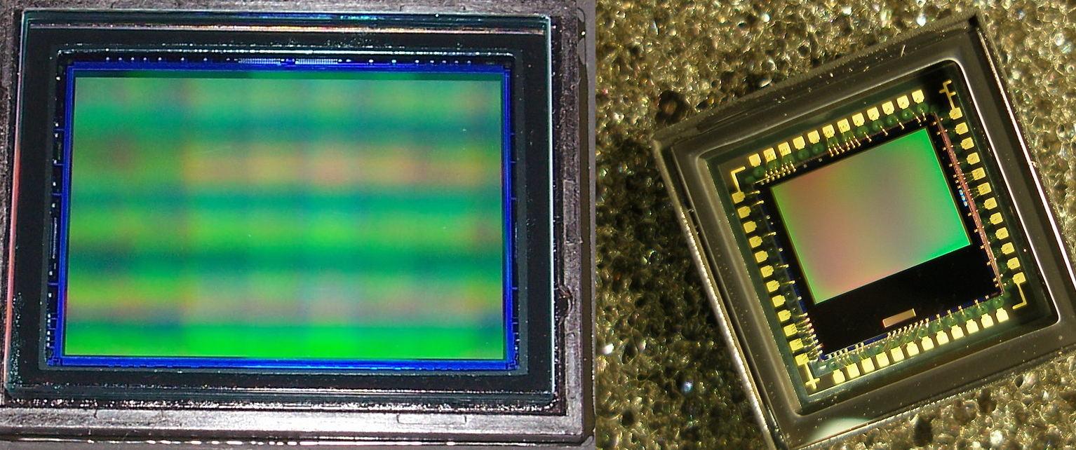
Because the CMOS imager is made using the same techniques as the vast majority of other chips, it benefits directly from advances in IC manufacturing. Another huge benefit is the ability to integrate the entire chip in one package, one wafer, one production line. This drives the cost for a CMOS solution way down, and the size, as well. The picture at the top of the post shows a CCD (left) and a CMOS sensor (right), for comparison. You can see the extra circuitry around the perimeter of the imaging section of the CMOS device, which is absent on the CCD.

Image courtesy Wikimedia commons user Jonen CC A-SA 3.0
In the picture above, you can see how the helicopter’s blades appear warped and misshapen while the rest of the image looks normal. The blades were moving fast enough relative to the capture times of the various pixels that different pixels caught the blades in different positions, creating the illusion of a physical warping.
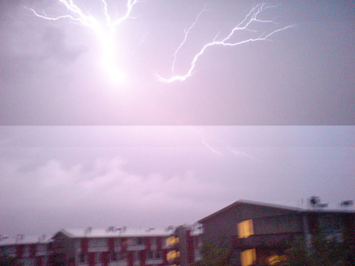
Image courtesy Wikipedia user Kalleboo CC A-SA 3.0
Here, you can see what happens when the illumination of a scene changes dramatically in the middle of image capture. Half of the image is significantly brighter because of the lightning.
Finally, the video above shows me playing with a Van De Graaf generator and a fluorescent bulb. Each time the charge builds up sufficiently to jump to the tube, the tube briefly lights up. As I turned my camera from landscape to portrait, you can see that the tube flashes all at once when it’s horizontally oriented, but appears to flash almost bottom to top when it’s vertically oriented. The horizontal pixels are captured fairly closely in time to one another, but from top to bottom, the timing varies greatly, creating the illusion that the light moves when it is, in fact, the exposure “window” moving across the lit tube.
Digital imaging is a very complex subject, of course, and this brief introduction really fails to do it adequate justice. If there’s suitable interest, perhaps I’ll do a larger, more in-depth tutorial covering the topic. If you’ve got questions, I’ll attempt to address them in the comments.
Before I go any further, I’m going to issue a pre-emptive engineering-lawyer warning: Some of the stuff I say here is going to be a gross oversimplification, and some of it, almost (but not quite) flat out wrong, but useful as a model for understanding the concept.
Images (left) courtesy Wikimedia Commons User Anderzej w k 2, CC BY-SA 4.0, and (right) courtesy Wikimedia Commons User Filya1, CC BY-SA 3.0
Types of Imaging Sensors
Imaging sensors are based on one of two technologies, CMOS or CCD. Each has its advantages and disadvantages, and with modern technology, it’s not really appropriate to say one is flat-out better than the other.I’ll also point out that there isn’t really such a thing as a “color” sensor – all imaging sensors simply record the number of photons striking some region of an object during a given time frame, irrespective of the color of those photons. To get a color image, filters are laid over the individual sensor regions to exclude certain wavelengths from those regions, and then the resulting data is extrapolated from neighboring pixels, which each allow different wavelengths to be recorded. The variety of methods with which this can be achieved could be an article unto themselves; I’m just going to stick to un-filtered (grayscale) imagers for the rest of the post.
CCD Imaging Sensors
The first truly successful imaging sensors were CCD type. CCD stands for “Charge Coupled Device,” which isn’t really all that useful.A very useful mental model for a CCD array is a line of people holding buckets, standing in a rainstorm. Let’s say you want to characterize how much water (light) is falling on an area. A way to do this would be to gather up, say, 300 of your closest, most patient friends, give all of them a bucket, 2/3 of them umbrellas, and have them form a rectangle 10 rows high and 30 columns wide. You’ll also need a megaphone. We’re also going to count off these poor shmucks, giving the ones without umbrellas the number one, then two and three, repeating.
In a CCD imager, there’s a very similar situation going on, where you have regions of the device that are exposed (no umbrella), and regions that are covered. The exposed regions gather light, turning photons striking the surface into electrons and storing them up during the “exposure” phase. During the “readout” phase, those electrons are passed along from one region (bucket) to the next until they reach the location where the analog-to-digital converter (ADC) is located, where the value is digitized. Here’s an excellent animation showing this process of scooting the charge across from one region to the next.
Animation courtesy Wikipedia User Schmid CC BY 2.5
Drawbacks to CCD Sensors
Complexity - One of the major drawbacks of the CCD is that it requires substantial external circuitry to operate. Because the nature of the semiconductor materials required to realize a CCD is different to those used for other types of integrated circuits, all of the control circuitry required must be located on other chips. Frequently, in addition to the timing signals required to synchronize the transfer of charge from one cell to the next and the ADC required to digitize the data, voltages outside of the normal battery range for mobile devices (~3-6V) are required, so those voltages must be created by large, expensive additional circuits.Smear - Smear happens when a bright light saturates cells on the imager. Its cause varies based on the readout type of the CCD (another very complex topic), and CMOS imagers aren’t susceptible to this type of artifact. You can see a good example of smear in this video of a Flaming Lips concert; compare that to this video of the same show, from a similar angle, but shot with a CMOS imager. You’ll see that the same light flashing causes a smear in the first video, but not in the second.
Thermal noise - Heat causes noise in CCD sensors, too; the warmer the image, the more free electrons there are just floating around in the semiconductor, messing up the image. Keeping an imager cool using thermoelectric coolers, liquid nitrogen, or other means is often used for high performance imaging applications. In particular, CCD sensors with aggressive active cooling find a great deal of application in super long exposure astronomy.
CMOS Sensors
Newer to the application is the CMOS imager. CMOS stands for “complementary metal-oxide semiconductor,” and unlike CCD, it’s not unique to imaging – most ICs these days are made with CMOS processes.If we’re going to keep with our “field full of friends” mental model, a CMOS imager has nobody covered by an umbrella. You can see right away that this provides an advantage; the active area of the imager can be smaller for a similar pixel count than with a CCD. Also, instead of passing the electrons from cell to cell to a converter, the CMOS sensor multiplexes the ADC internally to each pixel. The method of charge creation is different, as well: in a CCD, the region capturing light also stores the charge developed by the photons hitting the surface. In a CMOS imager, the light strikes a conventional photodiode and the current released from that interaction is stored in a capacitor.
Because the CMOS imager is made using the same techniques as the vast majority of other chips, it benefits directly from advances in IC manufacturing. Another huge benefit is the ability to integrate the entire chip in one package, one wafer, one production line. This drives the cost for a CMOS solution way down, and the size, as well. The picture at the top of the post shows a CCD (left) and a CMOS sensor (right), for comparison. You can see the extra circuitry around the perimeter of the imaging section of the CMOS device, which is absent on the CCD.
Drawbacks to CMOS Sensors
Rolling shutter - The biggest drawback to CMOS imagers is that most of them use a “rolling shutter” method of capturing the image. This means that not all of the image elements capture data at the same time; basically, pixels are captured sequentially, with pixels next to each other being captured relatively closely in time to one another but pixels at the top of the image are captured substantially later than pixels at the bottom of the image.
Image courtesy Wikimedia commons user Jonen CC A-SA 3.0
In the picture above, you can see how the helicopter’s blades appear warped and misshapen while the rest of the image looks normal. The blades were moving fast enough relative to the capture times of the various pixels that different pixels caught the blades in different positions, creating the illusion of a physical warping.

Image courtesy Wikipedia user Kalleboo CC A-SA 3.0
Here, you can see what happens when the illumination of a scene changes dramatically in the middle of image capture. Half of the image is significantly brighter because of the lightning.
Digital imaging is a very complex subject, of course, and this brief introduction really fails to do it adequate justice. If there’s suitable interest, perhaps I’ll do a larger, more in-depth tutorial covering the topic. If you’ve got questions, I’ll attempt to address them in the comments.
Subscribe to:
Posts (Atom)